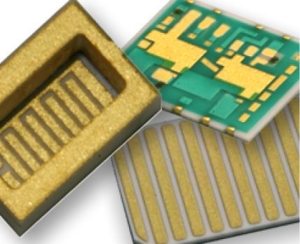
Leadless Ceramic SMT Substrates and Interposers
Remtec Product
Optimal Economy, Performance, and Reliability for SMT Packaging
Remtec’s ceramic leadless SMT substrates, chip carriers, and packages for direct PCB mounting utilize our proprietary Plated Copper on Thick Film (PCTF®) technology to create cost-effective solutions to house active and passive RF and microwave components, as well as multichip modules.
Typical applications include RF power amplifiers, MMIC modules, encoders, optical drivers, attenuators, filters, and transmit-receive modules—for telecom, satellite, optical network, WiMAX, and other communication markets, as well as for radar, military, and aerospace purposes.
Features
- Copper metallization, copper-plated solid plugged via holes, and PCTF wraparounds (castellations) suitable for RF signal transmission.
- Direct soldering of large leadless ceramic surface-mountable RF modules (greater than 0.75″ on a side) onto PCBs.
- Excellent solderability with the capability of withstanding multiple and prolonged soldering operations at 300°C and higher.
- Compliance with RoHS soldering requirements without any degradation in package integrity and reliability.
- Consistent dielectric properties, enhanced thermal management, and improved reliability.
- Packaging options in quantities of a few thousand parts per year up to 100,000 parts per month.
- Large panel, multiple array format for automatic assembly, significantly reducing the cost of PCTF substrates and packages.

Contact
We’re Ready to Help You.
Remtec’s team of technical experts will assist you with your metallized ceramic requirements. We provide a complete solution—from prototype design and fabrication to high volume production.
Please send your electronic files in DXF and/or DWG formats to sales@remtec.com. Additional design guidelines are available upon request.