About Us
Backed by a legacy of quality engineering, Remtec can deliver a creative, cost-effective metallized substrate and packaging solution designed to any specification.
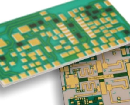
For more than three decades, Remtec has been a premier designer and manufacturer of thick film, direct bond copper substrates and packaging products for the electronics industry. We now lead the industry in specialty metallized applications with our advanced ceramic packaging technology: Plated Copper Thick Film (PCTF®).
Engineered specifically for electronics applications involving high power, heavy circuit density, and rigorous environmental conditions, our proprietary technology plates copper images over thick film on ceramic substrates.

In addition to ceramic substrates, Remtec designs and fabricates a wide range of metallized products utilizing our PCTF® technology, including chip carriers, hermetic and non-hermetic ceramic SMT packages, and other specialty components—all manufactured right here in our US-based facility.
Our patented manufacturing processes enable us to achieve a more uniform product with consistent yield, greater reliability, and higher performance results—every time.
Remtec is ISO 9001:2015 certified, RoHS and ITAR compliant.
Industries We serve

Military
PCTF®, AgENIG® and DBC for radar, flight guidance, navigation and target acquisition systems utilizing heat spreading package solutions for GaN semiconductors and RF & Microwave circuits.

Aerospace

Industrial Electronics
PCTF®, AgENIG® and DBC for laser submounts, and sensing/control functions.

Semiconductor Equipment
PCTF®, AgENIG® and DBC for high power RF Power Generators, high current carrying substrates, low inductance planar coils and precision matched resistors.

Opto Electronics

Medical Instrumentation
PCTF®, and AgENIG® for blood analyzers, dental x-rays, pulse oximeters, electronic surgical devices, implantable sensors, laser aesthetic solutions and scanning applications.

Transportation
DBC, AMB and PCTF® in high power, sensing and control in automotive and rail braking, traction control, charging, and LED lighting.

Commercial Telecom
PCTF® and DBC for high density optical packaging solutions, heat spreaders, RF test & instrumentation, and DC power circuitry where limited space and (SMT) surface mount solutions.
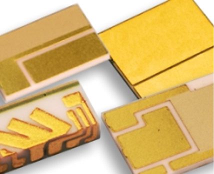
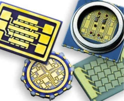
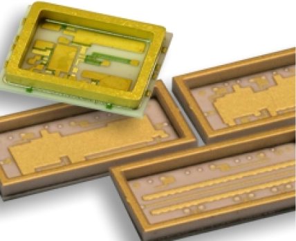
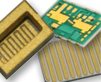
Remtec Products
Remtec offers a full range of thick film and direct bond copper (DBC) products, as well as customized solutions designed to any specification.
Products utilizing our proprietary Plated Copper Thick Film (PCTF®) technology achieve results not found with conventional thick films or co‐fired ceramics. Additionally, Remtec’s proprietary processes for electrolytic copper, nickel, gold, gold-tin, electroless nickel, and AgENiG provide finishes that are wire-bondable and solderable for even more options and flexibility.
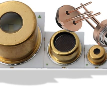
Laser & Photodiode Submounts
High-performance, cost-effective submounts, accessory circuits, and spacers manufactured to exact specifications.
LED Substrates & Submounts
Metallized substrates and submounts deliver economical packaging solutions for the most demanding applications.
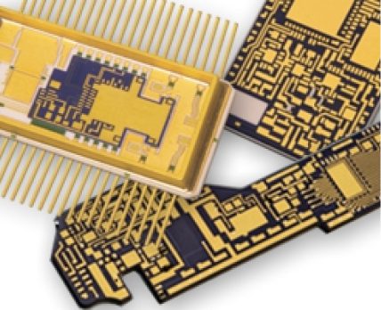
Leadless Hermetic & Non-Hermetic SMT Packages
Surface-mount technologies are a cost-effective alternative to standard TO-style packages for optoelectronics, offering optimal reliability and high-performance features, at a lower cost and faster time-to-market.
Leadless Ceramic SMT Substrates & Interposers
Substrates, chip carriers, and packages, designed and manufactured for direct mounting of components and multichip modules.
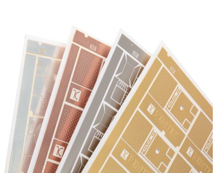
Low-Cost AgENIG Substrates
Innovative substrates provide RoHS compliance without expensive platinum and palladium films.
Metallized Ceramic Sensors
Superior protection for delicate sensor and detector components operating in harsh environmental conditions.
High-Density Thick Film Substrates
Thick film ceramic circuits are precision-engineered for cost versatility, reliable performance, and flexible design options.
DBC and AMB Substrates
DBC substrates feature excellent solderability, better thermal conductivity, and higher current capacity—at a lower cost.
News + Events
Here’s what we’re talking about at Remtec.
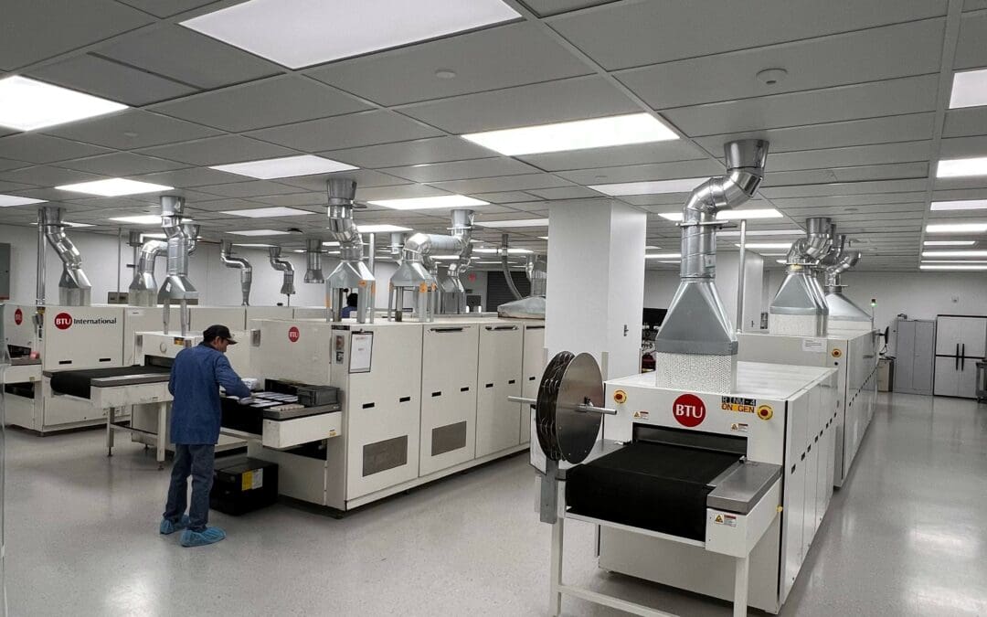
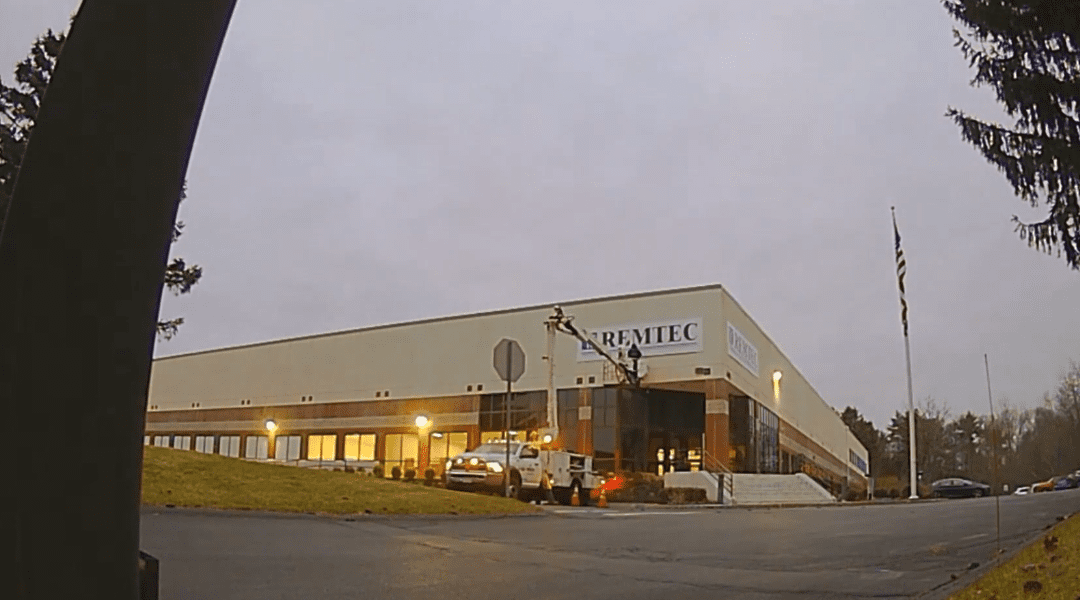
Remtec Announces Completion and Transition to its new 55,000 sq. ft., $12+ million facility in Canton, MA
Canton, MA -- Remtec Incorporated -- a leading U.S. provider of ceramic-based packaging, assemblies, substrates, and components applied across the electronics industry announced today that, after a year-long construction project, it has completed its new, 55,000 sq....
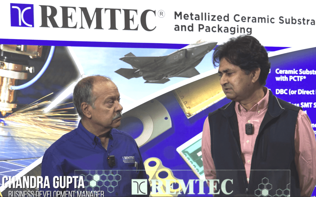
Remtec’s Chandra Gupta highlights ceramic technology at APEC 2024
At APEC 2024 in Long Beach, CA, Remtec’s Business Development Manager, Chandra Gupta, had an opportunity to speak at the Remtec booth...

Remtec awarded $150k grant from Workforce Training Fund Program (WTFP) distributed by Massachusetts’ Healey-Driscoll administration
Recently relocated in a newly renovated facility in Canton, MA -- Remtec will use the grant to invest in its people and competitiveness, just in time to take advantage of re-onshoring trends in US electronics industry. Canton, MA -- Remtec Incorporated -- a leading...
Remtec’s final, pre-opening time-lapse clips from its new Canton, MA facility
Here is the final time-lapse footage from Remtec's new-facility construction project in Canton, MA (recorded October...
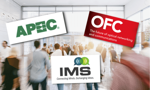
Remtec announces participation in 2024 trade shows
Remtec is excited to announce three key 2024 trade shows in which it will participate. At a high level -- and noting more details and information will be available for each show as the show-dates approach -- here is a summary of the events we'll be attending as an...